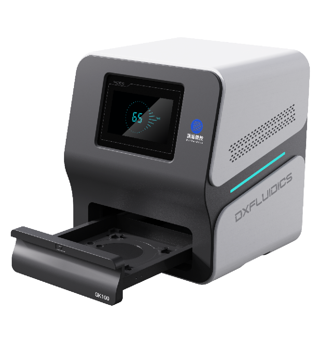
GK-100紫外接触式光刻机
顶旭桌面微型光刻机GK-100,专为微米级图案制作而设计,旨在保障卓越的图形转移精度。设备采用紫外LED冷光源,结合双非球面石英透镜,可生成半角<2°的平行光,相较传统接触式曝光机,其极致紧凑的体积将移形换影置于桌面之上,为操作提供了便利与精准。
Product Details
Desktop microlithography, designed for micron-level patterning, is designed to guarantee superior graphic transfer accuracy.
The equipment adopts UV LED cold light source, combined with double aspherical quartz lens, can generate parallel light with half angle <2°, compared with the traditional contact exposure machine, its ultra-compact volume will be shifted above the desktop, providing convenience and precision for operation.
The photolithography machine is widely used in the preparation of microfluidic chips, MEMS devices, optoelectronic devices and surface acoustic wave devices. Its performance is especially suitable for universities, research institutes and enterprises to carry out microfabrication process research.
Following the pace of modern technology, the introduction of Top Asahi's desktop microlithography has injected new vitality into micro and nanoprocessing, helping customers to move towards higher precision and innovation in the realization of their project goals.
1. Technical parameters
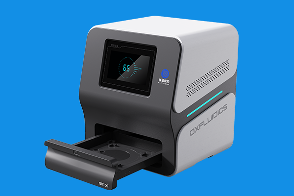
- Exposure Light Source: UV LED
- Wavelength of Light Source: 365nm
- Exposure Area: 4 inches, 6 inches optional
- Exposure Method: Single-side contact timed exposure
- Exposure Resolution: 2um
- Exposure Intensity: Adjustable from 20 to 200mW/cm22可调;
- 曝光不均匀性:≤10%;
- 光源平行性:≤5°;
- Light Source Lifespan: ≥20,000 hours
- Power Supply Input: AC 220V ±10V, 50Hz
- Power Consumption: 250W
- Weight: 25kg
- Dimensions: 382 (Length) * 371 (Width) * 435 (Height)
- Operating Environment: Temperature 0℃-40℃, Relative Humidity <80%
2. Methods of use
This equipment is easy to operate and user-friendly. The specific operations are as follows:
I. Preparations Before Exposure
1、硅片处理:确保待曝光硅片经过匀胶处理,表面干净平整,没有明显的污渍或破损。
2、选择光刻板:根据项目需要,选择合适尺寸的光刻板,本设备兼容4英寸、5英寸或6英寸。
3、设备检查:仔细检查设备,确保所有部件处于正常工作状态,确保操作环境良好。
II. Exposure Operation Steps
1、安装硅片:将待曝光硅片平放在设备的载台上,确保位置准确。
2、放置光刻板:2)Position the Photomask: Place the photomask flat above the silicon wafer. If using film masks, transparent glass should be positioned above to maintain stability.
3、设定曝光参数:使用控制面板设置曝光时间和强度,根据具体需求进行调整。
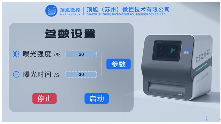
(Save Exposure Parameters: The parameter function allows the convenient saving of commonly used exposure parameters for easy retrieval during usage.)
4、启动曝光:确认参数设定无误后,点击启动按钮,设备将开始进行曝光。
5、监控曝光过程:在曝光过程中,您可以通过设备界面监控曝光进度,确保一切顺利进行。
6、曝光完成:Exposure Completion: Once the exposure is complete, the equipment will provide a prompt. Remove the silicon wafer and the photomask.
Contact Information









 ZH_CN
ZH_CN  EN
EN